Ipc 7351
Your component footprint is more than just a drawing on paper. And smart bulk editing tools.
Ipc 7351 Pcb Design Guidelines PCB Designs
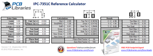
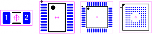
The suffixes 'l' and 'm' indicate least and most real estate on the pcb and the name with no suffix indicates nominal density on the pcb.
Ipc 7351. Pcb信仰工艺尺第三版 赠送配套讲解课程(该课程是 pcb设计一板即成功专栏的子集,内容会同步到pcb设计一板即成功专栏 )(¥29.9 包邮 持续供货中,如需一次性购买多把请联系老wu微信号:wcb_50470527获取优惠). Each pcb component manufacturer will publish a data sheet on the parts that they provide. They do not guarantee any supposed thermal properties, particularly as these are also strongly influen ced by many other parameters.
Still the given solder pad dimensions will be found adequate for most general applications part number and product description part number: In your cad software, it collectively includes your pcb land pattern, silkscreen markings, any solder mask opening, and component outline defined in the. 我们经过一段时间的调查发现 大部分的制图工程师 制作封装的依据是 ipc 7351.
Free access to over 10 million parts. In addition to the electrical and physical specifications in these data sheets, they often will include a recommended pcb layout land pattern as well.

PCB Land Pattern Design to the IPC7351 Standard

IPC7351 Footprint Wizard Layout KiCad.info Forums
IPC7351 Land Patterns OSH Garage

IPC7351 Footprint Wizard Layout KiCad.info Forums

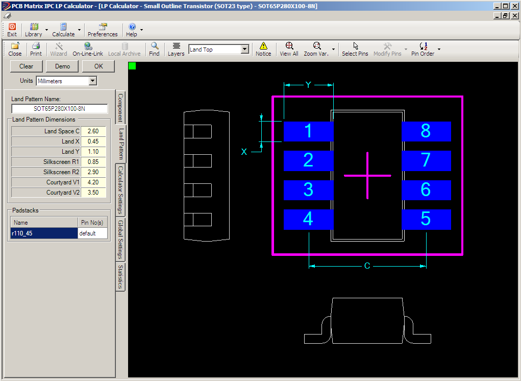
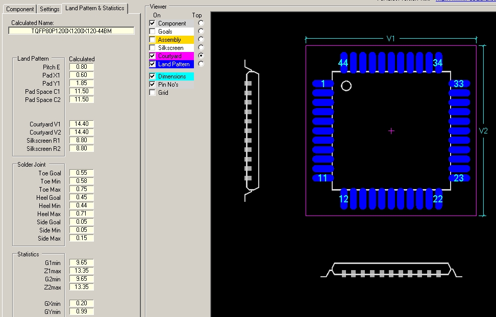
PCB_Matrix_IPC7351_LP软件介绍硬件开发文档类资源CSDN下载
Ipc 7351 Pcb Design Guidelines PCB Designs
IPC7351 Land Patterns OSH Garage
Ipc 7351 Pcb Design Guidelines PCB Designs

Free IPC7351 Land Pattern Calculator MightyOhm
IPC7351 LP Viewer10.2使用说明_廖旭 廊坊师范学院信息技术提高班第十一期CSDN博客


IPC7351 The IPC Standard for PCB Footprint Creation Tempo
Footprints diverser Bauteile
IPC 7351B DOWNLOAD
The IPC7351 Specification Explained SOIC Components SnapEDA Blog
ipc7351电子发烧友网

IPC 7351A PDF DOWNLOAD
IPC7351 LP Viewer10.2使用说明 CSDN博客

IPC7351 Padstack Naming Convention PCB Libraries Forum Page 3
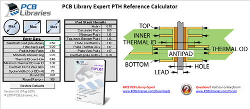
IPC7351 SMD & PTH Reference Calculators PCB Libraries Forum Page 1